As the core equipment for ultra-thin material processing, capacitor film slitting machine is widely used in the field of precision electronic film (such as MLCC dielectric film, lithium battery separator, flexible circuit substrate, etc.). The following is a professional analysis from three aspects: technical characteristics, application scenarios and industry trends:
First, analysis of technical advantages
1. Nanometer slitting accuracy
◦ The air bearing spindle (radial runout ≤1μm) and laser interferometer closed-loop control are used to achieve 0.5μm slitting accuracy, which meets the processing needs of ultra-thin polyimide (PI) film and PET film below 2μm.
◦ Active tension control system (fluctuation ±0.5N) with ultrasonic edge detection to avoid film stretching and deformation.
2. Multiphysics collaborative machining
◦ Integrated cold knife slitting (-30°C low temperature treatment) and laser micro edging technology to solve the problem of thermal deformation of polymer materials, and the cut roughness reaches Ra0.2μm.
3. Intelligent compensation system
◦ Machine vision-based in-line thickness monitoring (resolution 10nm) with adaptive tool wear compensation ensures consistent batch machining.

Second, typical application scenarios
| Fields of application | Type of material | Technical Indicator Requirements | Solution Highlights: |
| MLCC dielectric film | Modified BaTiO₃/PVDF composite membrane | Width tolerance ± 3μm, burr-free | Magnetic levitation slitting + plasma edge passivation |
| Lithium battery separator | Three-layer PP/PE/PP | Microporous structure protection (pore size≤ 100nm) | Low-temperature plasma-assisted slitting technology |
| Flexible OLED substrates | Transparent polyimide film | The surface resistance fluctuates ≤ 5 Ω/sq | Vacuum adsorption transmission + ionized air dust removal system |
Third, cutting-edge technology trends
1. Quantum dot film processing
For the CdSe quantum dot film for QLED display, an ultraviolet laser protection slitting process (wavelength 355nm, pulse width 15ps) was developed to avoid the photodegradation of quantum dot materials.
2. Ultra-thin copper foil treatment
The slitting of 6μm electrolytic copper foil uses a nano-diamond-coated tool (cutting edge radius 50nm) and hydrogen-helium mixed gas protection to achieve curl-free cutting.
3. Digital twin system
Predicting tool life with real-time digital mirroring (sampling frequency 1kHz) reduces unplanned downtime by up to 70%.
Fourth, industry challenges and development
• Bottleneck: Single-layer slitting of 2D materials such as graphene still has edge lattice damage (defect density> 10³/cm²)
• Innovation direction:
◦ Atomic layer etching (ALE) technology is a composite process of mechanical slitting
◦ Terahertz band on-line detection system (0.1-10THz)
With the explosion of emerging demand for 5G/6G high-frequency substrate materials and perovskite photovoltaic films, the next generation of slitting machines will develop in the direction of "atomic-level precision + AI real-time control", and the global market size is expected to exceed $2.8B (CAGR 11.3%) in 2026.
The tool holder driven by servo motor can achieve a positioning accuracy of ±0.01mm, reducing the burr on the edge of the film.
21. June, 2025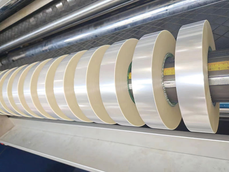
It has evolved from a single processing equipment to an intelligent production unit integrating perception, decision-making and execution.
20. June, 2025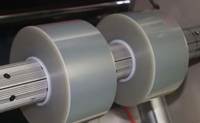
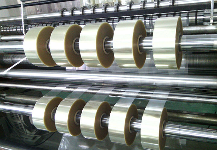
high-precision slitting (accuracy ± 1μm) and tension control (±0.5N) ensure that the film is not damaged.
18. June, 2025The key to improving the productivity of capacitor film slitting machines is to optimize the tool change process and realize automatic adjustments
17. June, 2025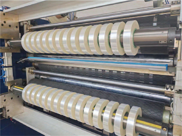
industrial-grade touch screen (IP65 protection) adapts to the high dust environment of the film slitting workshop.
16. June, 2025


